Memory, Maps, and Mayhem - Day 3: Intro to Computer Architecture - Part 2

Day 3 of Infineon's course was a journey into the heart of the machine. With Prakash sir as our guide, we explored the intricate world of memory architectures, cache performance, and the high-speed interconnects that tie it all together.

After two days of setting the stage, Day 3 plunged us into the very core of how an embedded system thinks and remembers. Guided by the expertise of Prakash sir, we peeled back the layers of abstraction to understand the intricate dance of memory and data that happens every microsecond.
Dissecting a Program's Memory
We started by looking at a simple piece of C code to answer the question: when you write a program, where do all the variables and instructions actually live?
// main.c
const int LOOP_COUNT = 5;
int a[5] = { 20, -19, 773, 47, -146};
int b[5];

void main(void){
    int *ptr;
    ptr = b;
    while(port->portA==0){
        for(int i=0;i<LOOP_COUNT;i++){
            ptr[i] = a[i];
        }
    }
}
It turns out the compiled program is neatly organized into different segments, each with a specific purpose:
.textsection: Stores the executable code, themain()function itself. It's typically read-only..rodata(Read-Only Data) section: Home for constants that never change, like ourLOOP_COUNTvariable..datasection: Contains global and static variables that are initialized with a value, like our arraya..bss(Block Started by Symbol) section: A special place for global and static variables that are uninitialized, like arrayb. The system ensures they are zeroed out before the program starts.- Stack: Used for local variables, like
ptr, and for managing function calls. It grows and shrinks as needed.
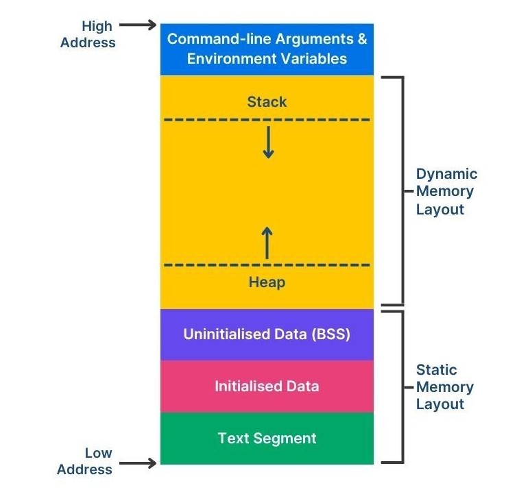
Figure 1: How a simple C program is mapped into different memory segments.
The Memory Landscape: Volatile vs. Non-Volatile
Not all memory is created equal. The most fundamental division is based on what happens when the power goes out:
- Volatile Memory: Forgets everything when powered off. It's fast and ideal for temporary storage.
- SRAM (Static RAM): Incredibly fast because it's built from flip-flops. It doesn't need refreshing but is expensive and power-hungry. Perfect for CPU caches.
- DRAM (Dynamic RAM): Uses tiny capacitors to store bits. It's cheaper and denser than SRAM but needs to be constantly refreshed to retain data. This is your computer's main RAM.
- Non-Volatile Memory: Remembers its data even with no power. It's essential for storing the program itself and permanent data.
- Flash Memory: The workhorse of modern electronics. It comes in two main flavors:
- NOR Flash: Allows for fast, random-access reading, making it ideal for executing code directly from it (Execute-In-Place).
- NAND Flash: Offers faster write/erase speeds and higher density, making it the choice for data storage, like in SSDs and SD cards.
- Flash Memory: The workhorse of modern electronics. It comes in two main flavors:
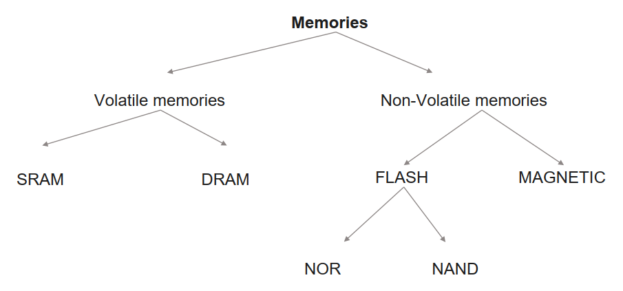
Figure 2: The family tree of memory technologies.
Multi-Core Memory Architectures
In a system with multiple CPUs, how they access memory is a critical design choice.
-
Shared Memory: All CPUs share a single global memory space.
- UMA (Uniform Memory Access): The simplest model. Access time to any memory location is the same for all CPUs. Think of it like a small round table where everyone can reach the salt shaker equally easily.
- NUMA (Non-Uniform Memory Access): Access time depends on the memory's location relative to the CPU. A CPU can access its own "local" memory much faster than "remote" memory attached to another CPU. This is like a long banquet table—it's much faster to grab what's in front of you.
-
Distributed Memory: Each CPU has its own private memory island. There is no shared space; they communicate by sending messages over a network.
Most modern, complex systems use a Hybrid model, combining these approaches.
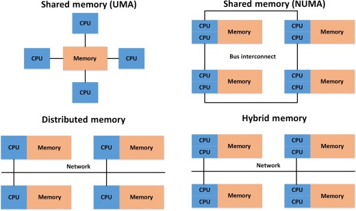
Figure 3: Uniform Memory Access (UMA), Non-Uniform Memory Access (NUMA), Distributed and Hybrid.
The Microcontroller Memory Hierarchy
Prakash sir then showed us how this applies to a real microcontroller. The memory isn't one big block; it's a hierarchy of layers, each faster and smaller than the last.
- Level 0 (L0): The CPU's personal caches. Blazing fast.
- Level 1 (L1): Closely-Coupled Memories (CCMs). These are small, fast SRAMs physically located right next to each CPU core. This is a NUMA setup because CPU-1's L1 memory is local to it but remote to CPU-2.
- Level 2 (L2): A larger shared memory that all CPUs can access. Since it's a common resource, the access time is roughly the same for all cores, making it a UMA system.
Even though L1 memories are local, they often exist in a global address map. This means CPU-2 can access CPU-1's L1 memory, but it will be a slow, inefficient operation. However, truly private memory regions can be configured to be completely invisible and inaccessible to other cores.
Caches: The Need for Speed ⚡
Why do we even need this complex hierarchy? Because CPUs are ridiculously fast, and main memory is tragically slow. A CPU waiting for data is a wasted CPU. Caches bridge this speed gap based on two principles of locality:
- Temporal Locality: If you access a piece of data now, you're likely to access it again soon.
- Spatial Locality: If you access a memory location, you're likely to access its neighbors soon (e.g., iterating through an array).
When the CPU requests data from an address, the cache doesn't just fetch that one piece of data. It performs a Cache Line Fill, grabbing a whole block of adjacent memory. Now, when the CPU needs the next piece of data, it's already in the super-fast cache—a cache hit! This dramatically reduces the time spent waiting on slow main memory.
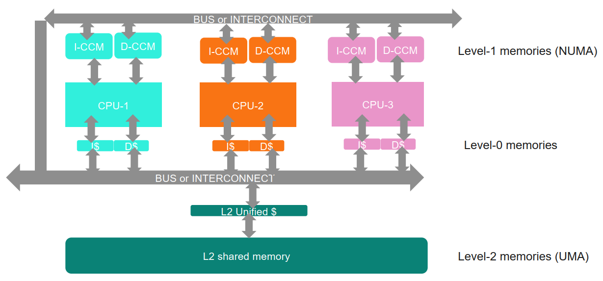
Figure 4: The cache acts as a high-speed buffer, satisfying most of the CPU's requests to avoid trips to slow main memory.
Connecting it All: The Interconnect
With all these CPUs, memories, and peripherals, how do they talk to each other? Through an Interconnect.
We started with a Shared Bus, where everyone is connected to a single set of wires. It's simple, but only one "master" can talk at a time. An Arbiter acts as a traffic cop, managing access with bus request and bus grant signals.
A more sophisticated approach is a multi-level bus structure. High-performance components (like CPUs and memory) sit on a fast bus like AHB (Advanced High-performance Bus). Slower peripherals (like GPIO) sit on a low-power APB (Advanced Peripheral Bus). A Bridge connects the two, translating transactions between them.
But for true parallel performance, we need a Crossbar Switch. This is like a dedicated telephone exchange. It creates direct, simultaneous connections, allowing CPU-1 to write to Flash at the exact same time a DMA controller is moving data from a sensor to RAM.
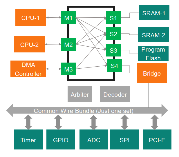
Figure 5: A Crossbar Switch enables multiple, concurrent data transactions, unlocking the full power of a multi-master system.
The Grand Finale: Our PSoC!
The day concluded by looking at the block diagram of the PSoC 4100S Plus, the very microcontroller we will be working on! It was the perfect "Aha!" moment. We could see the Cortex-M0+ CPU, the Flash and SRAM, the AHB and APB buses, the DMA, and all the peripherals. All the abstract concepts from the day suddenly clicked into place on a real, tangible piece of hardware.
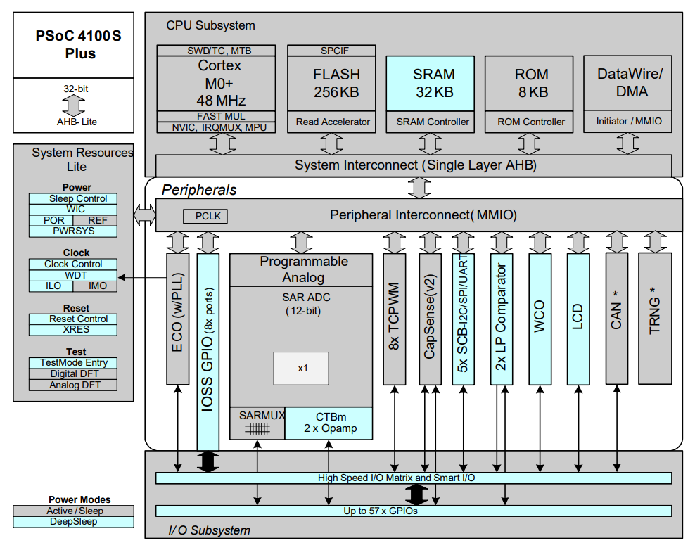
Figure 6: The block diagram of the PSoC 4100S Plus.
Day 3 was an intense but incredibly rewarding exploration. We journeyed from a single line of C code down to the fundamental hardware architecture and back up again.
#Infineon #EmbeddedSystems #Cohort3 #ComputerArchitecture #MemoryHierarchy #Cache #Interconnect #PSoC #NUMA #AHB